
About Us
Engineering the Future of Advanced Semiconductor Packaging
From silicon photonics and co-packaged optics to 3D SiP modules and power electronics - India's only dedicated advanced packaging facility, backed by three decades of electronics engineering heritage.

+
Photonic Chip Packaging Initiative
Advancing Next-Generation
Photonic Processors
A Division of izmo Limited,
Headquartered in Bangalore
izmo Microsystems (izmomicro) is the advanced semiconductor packaging division of IZMO Limited, listed on the National Stock Exchange (NSE) of India. With over three decades of expertise in electronics design and manufacturing, izmomicro focuses exclusively on next-generation System-in-Package (SiP) and IC packaging technologies.
Operating from a state-of-the-art Class 1000 cleanroom facility in Whitefield, Bangalore, we serve clients across aerospace, defense, telecom, automotive, data center, and industrial sectors — delivering solutions from concept through volume manufacturing.
Enabling Next-Generation Semiconductor Packaging
Mission
To be India's premier advanced semiconductor packaging partner — bridging the gap between chip design and commercial deployment. We enable fabless semiconductor companies, research institutions, and system integrators to bring next-generation silicon to market with packaging solutions that meet the most demanding performance, reliability, and security requirements.
Vision
To establish India as a global hub for advanced semiconductor packaging innovation — developing indigenous capabilities in silicon photonics, co-packaged optics, 3D die stacking, and heterogeneous integration that rival the world's leading OSAT providers, while maintaining the agility and responsiveness of a specialized partner.
Led by Deep Domain Expertise
izmomicro's leadership and engineering teams bring decades of combined experience in semiconductor packaging, photonics, RF design, power electronics, and system integration. Our team includes specialists in die attach, wire bonding, flip-chip assembly, substrate design, thermal management, and photonic alignment - working alongside materials scientists, process engineers, and quality experts.
Backed by IZMO Limited's established electronics engineering heritage and strengthened by our partnership with IIT Madras, we combine academic research rigor with commercial execution capability - enabling us to take on the most complex packaging challenges across industries.
Packaging Design
SI/PI analysis, thermal simulation, substrate co-design, and DFM optimization.
Process Engineering
Die attach, wire bond, flip-chip, photonic alignment, molding & encapsulation.
Test & Qualification
JEDEC, AEC-Q100, MIL-STD reliability testing and failure analysis.
R&D Innovation
DSIR-recognized R&D with IIT Madras CPPICS partnership.
Local Expertise, Global Delivery
Engineering offices across three continents ensure local support and rapid response for clients worldwide.
Bangalore, India
HQ51, 52, KIADB Export Promotion Industrial Area,
Whitefield, Bangalore 560066, India
San Francisco, USA
251 Post St, Suite 412, San Francisco, CA 94108,
USA
Köln, Germany
Richmodstraße 6, 50667 Köln, Germany
Exclusive Industry Partner - IIT Madras Photonic Chip
Packaging Initiative
izmomicro is the exclusive industry partner of the Centre for Programmable Photonic Integrated Circuits and Systems (CPPICS) at IIT Madras. This collaboration bridges cutting-edge academic research with commercial-scale packaging capabilities — advancing programmable photonic processors (FPPGA), quantum photonic integration, AI-driven photonic systems, and silicon photonics for telecom and computing applications.
 IIT Madras
  CPPICS
 World-Class Infrastructure, Rigorous Standards

ISO 9001:2015
Certified quality management system ensuring consistent, traceable, and repeatable manufacturing processes for aerospace, defense, and high-reliability applications.

DSIR Recognition
In-house R&D unit recognized by the Department of Scientific & Industrial Research (DSIR), Government of India — affirming commitment to advanced packaging innovation.

Class 1000 Cleanroom
State-of-the-art cleanroom in Whitefield, Bangalore equipped for advanced die attach, wire bonding, flip-chip assembly, and photonic alignment processes.

JEDEC & AEC-Q100
Full qualification support for JEDEC and AEC-Q100 standards, meeting the reliability requirements of automotive, industrial, and consumer electronics markets.

IP Protection Protocols
Strict access controls, NDA-backed workflows, and compartmentalized project management safeguarding proprietary designs from concept through volume production.

IATF 16949 Ready
Processes aligned with automotive quality management standards, supporting the growing demand for automotive-grade semiconductor packaging in EV and ADAS applications.
Full-Spectrum Advanced Packaging
Under One Roof
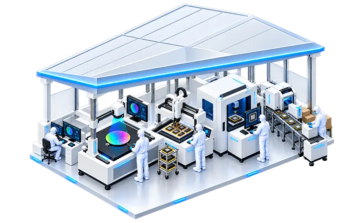
Our Whitefield facility houses comprehensive semiconductor packaging capabilities spanning the full product lifecycle — from design simulation through volume production.
- Silicon photonics & co-packaged optics assembly
- 3D die stacking & flip-chip BGA
- Fine-pitch wire bonding & hermetic sealing
- Power module assembly (DBC, DBA, AMB substrates)
- RF/microwave multi-chip module packaging
Join Our Team or Partner With Us
Whether you're a semiconductor professional looking to shape the future of advanced packaging, or a company seeking a dedicated packaging partner - we'd love to hear from you.
-
Packaging-centric ASIC design
-
Broad package portfolio
-
Comprehensive testing and qualification
-
Aligned ASIC, package & PCB for first-pass success