
Semiconductor Packaging & Photonics Engineering Blog
Blog & Insights
Technical insights on advanced semiconductor packaging, silicon photonics, co-packaged optics, and the technologies shaping next generation electronics.
 NEW BLOG
How Advanced Semiconductor Packaging is Driving the Next Generation of Electric Vehicles
From SiC power modules to integrated sensor arrays, advanced packaging is reshaping EV architecture. Explore how next-gen SiP solutions are enabling higher efficiency, longer range, and faster charging.
Read Article →
Smaller, Smarter, And Faster: How Advanced Packaging Is Powering Edge AI
Read More →
The Silicon Carbide Shift In Next Generation EV Design
Read More →
Connecting The EV Ecosystem With Next Gen RF Solutions
Read More →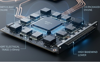
Why Silicon Photonics Shifts The Real AI Performance Bottleneck To The Package
Read MoreReady to Build What's Next?
Whether you're developing a silicon photonic transceiver, co-packaged optics module, or a novel photonic integrated circuit, our team provides end-to-end packaging support from design consultation through volume manufacturing.
-
Design & simulation support
-
Prototype through volume production
-
JEDEC & AEC-Q100 qualification
-
IP-secure packaging environment