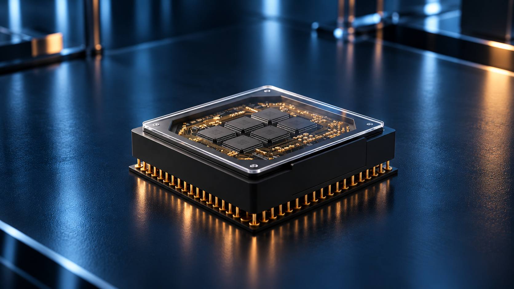


ASIC Packaging

ASIC PACKAGING SOLUTIONS

Custom IC Packaging for Peak Performance

Packaging-centric co-design for fabless ASIC firms. From architecture review through volume production, we deliver optimized electrical performance, thermal management, and signal integrity across QFN, BGA, flip-chip, and 3D SiP platforms.

Exploded view of a multilayer integrated circuit package on a circuit board
Min. Ball Pitch
0.4 mm
Max Die Size
40 mm
I/O Count
2500+
Qualification
AEC-Q100
Certified Facility
ISO 9001

WHY IZMO FOR ASIC

Packaging Excellence for ASIC Innovation

From early-stage architecture through volume production, we integrate packaging expertise into every phase of your ASIC development. Our concurrent co-design approach eliminates costly iterations and accelerates your time to silicon.

  • Packaging considerations integrated into ASIC architecture from project inception
  • Optimal electrical performance, thermal management, and signal integrity
  • Parallel ASIC, package, and PCB development for first-pass success
  • ISO 9001:2015 certified - commercial, automotive, aerospace & defense

IP SECURITY

Safeguarding Innovation & Intellectual Property

Advanced SiP packaging techniques create an inherent layer of IP protection by integrating complex systems into discreet, non-discernible modules.

Our IP-secured packaging environment ensures your proprietary designs remain protected throughout the development lifecycle - from initial concept through volume production.

PACKAGE TECHNOLOGIES

Package Technology Portfolio

A comprehensive spectrum of IC package formats engineered for performance, reliability, and manufacturability across every application domain.

QFN

LEAD-FREE

Quad Flat No-Lead

Compact, high-performance packages with excellent thermal and electrical performance in a near chip-scale footprint. Low-inductance ground connections via exposed pad for superior high-frequency operation.

Body (mm)
3*3 - 12*12
Pitch (mm)
0.4 - 0.65
Lead Count
4 - 88
Profile
0.85 mm
COMPACTLOW PROFILETHERMAL PAD

BGA

SUBSTRATE

Ball Grid Array

Industry-standard substrate-based packaging supporting fine-pitch routing and multi-layer signal distribution. High I/O density with superior thermal dissipation through solder ball array.

Body (mm)
0.5 - 1.27
Max I/O
2500+
Substrate
Organic/LTCC
Routing
Multi-layer
HIGH I/OFINE PITCHTHERMAL

CSP / WLP

WAFER LEVEL

Chip Scale / Wafer Level Package

Near-die-size packaging enabling the smallest possible form factor with direct board-level solder attach. Fan-in and fan-out WLP options for mobile, wearable, and IoT applications.

Pitch (mm)
0.3 - 0.5
Footprint
1.2x die
WLP Types
Fan-in/out
Profile
<0.5 mm
MIN FOOTPRINTWAFER-LEVELIOT

Flip Chip BGA

HIGH PERFORMANCE

Controlled-Collapse Chip Connection

Direct die attach for lowest inductance and highest-speed performance. Cu pillar or solder bump technology for superior signal integrity and power delivery at multi-GHz frequencies. Ideal for HPC, networking, and RF.

Bump Type
Cu Pillar
Bump Pitch
<100 µm
Max Die
40 mm
Frequency
Multi-GHz
LOW INDUCTANCEHIGH SPEEDHPC

3D SiP

MULTI-DIE

Three-Dimensional System-in-Package

Multi-die stacking with through-silicon vias or wire bond interconnects for heterogeneous integration of digital, analog, and sensor functions in a single package footprint.

Interconnect
TSV / WB
Stack Height
2-8 die
Technology
Mixed
Integration
3D
HIGH I/OFINE PITCHTHERMAL

Specialized IC

CUSTOM

Custom & Application-Specific Packages

Tailored packaging solutions for unique requirements including hermetic seal, ceramic cavity, open-cavity QFN, and HTCC/LTCC substrates for aerospace, defense, medical, and sensor applications.

Seal Type
Hermetic
Substrate
Ceramic
Qualified
MIL-STD
Form Factor
Custom
HERMETICAEROSPACEDEFENSE

STRATEGIC PARTNERSHIP

Exclusive Industry Partner IIT Madras Photonic Chip Packaging Initiative

Collaborating on programmable photonic processors (FPPGA), quantum and AI-driven photonic integration, and silicon photonics for telecom and computing - bridging academic research with commercial-scale packaging.

SI / PI Analysis

Full-wave electromagnetic simulation of signal integrity and power delivery networks across package and PCB.

Thermal Management

CFD-based thermal simulation and heat spreader design for high-power ASIC applications.

Substrate Design

Multi-layer organic, LTCC, and HTCC substrate layout with fine-pitch routing and via optimization.

DFM / DFT

Design for manufacturability and testability reviews ensuring production-ready package designs.

QUALITY & RELIABILITY

Rigorous Testing & Qualification

Every ASIC package undergoes comprehensive reliability qualification protocols to meet the most demanding industry standards. Our testing framework covers the full spectrum of environmental, mechanical, and electrical stress conditions.

  • Thermal cycling (-65°C to +150°C)
  • JEDEC JESD22 compliance
  • Board-level reliability (BLR)
  • X-ray & acoustic inspection
  • HAST / uHAST humidity testing
  • AEC-Q100 automotive grade
  • Mechanical shock & vibration
  • Custom mission-critical protocols

END-TO-END SUPPORT

From Concept to Volume Production

Our integrated approach ensures seamless progression through every stage of ASIC packaging development.

  1. PHASE 01
    ARCHITECTURE

    Package Co-Design

    Collaborative design of ASIC, package substrate, and PCB in parallel. Signal integrity, power delivery, and thermal analysis from the earliest stages to eliminate costly respins.

  2. PHASE 02
    VALIDATE

    Prototyping & Qualification

    Rapid prototyping with full JEDEC and AEC-Q100 qualification testing. Comprehensive reliability validation including thermal cycling, HAST, and board-level reliability assessment.

  3. PHASE 03
    PRODUCE

    Volume Manufacturing

    Scalable production from engineering samples through full-rate manufacturing. Consistent quality assured by ISO 9001:2015 processes and advanced in-line inspection systems.

Get Started

Discuss Your ASIC Packaging Needs

Partner with izmomicro for packaging-centric co-design that delivers first-pass success. From architecture review through volume production, we bring decades of ASIC packaging expertise to your project.

  • Packaging-centric ASIC design

  • Broad package portfolio

  • Comprehensive testing and qualification

  • Aligned ASIC, package & PCB for first-pass success