
Semiconductor Packaging Case Studies

PROVEN ENGINEERING SOLUTIONS

Case Studies

Real-world semiconductor packaging challenges solved for aerospace, defense, telecom, and industrial clients worldwide. From 84% footprint reduction to high-density RF boards and advanced thermal management.

Advanced semiconductor packaging for space technology
 
CASE STUDY

Revolutionizing Space Technology: Advanced Semiconductor Packaging for a Leading Space Agency

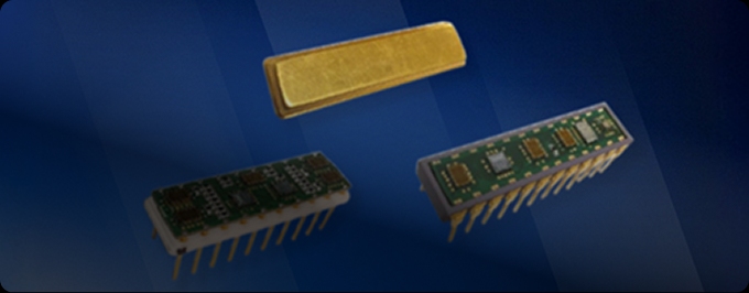
84% footprint reduction through 3D space-grade SiP module for satellite payload camera electronics. Multi-chip integration with hermetic packaging for extreme-environment operation.

Read full case study →
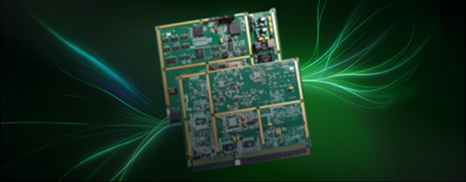
High-density RF SOC board
 
CASE STUDY

High-Density RF SOC Board for a Leading Wireless Telecom Solutions Company

Fine-pitch BGA assembly with controlled impedance routing for 5G applications.

Read full case study →
Thermal management engineering
 
CASE STUDY

Engineering for Endurance: Thermal Management for a Global Leader in 3D Printing

Custom DBC substrate and heat spreader design for continuous high-temperature operation.

Read full case study →
 CASE STUDY CASE STUDY

High-Density SBC VPX Board Design For A Government Research Lab

Multi-Layer HDI PCB With Ruggedized Connectors For Defense-Grade Computing Systems, Designed To MIL-STD Requirements.

Read full case study →
Technical Brief TECHNICAL BRIEF

Overcoming Obsolescence: A New Era For LVDT Signal Conditioning & Health Monitoring

Redesigned Legacy Analog Front-End Into A Compact SIP Module With Enhanced Reliability And Extended Lifecycle.

Read full case study →
 INDUSTRY REPORT INDUSTRY REPORT

From Legacy To Longevity: Solving Component Obsolescence For A Leading Aviation Electronics Manufacturer

Form-Fit-Function Replacement Packaging That Extended Product Life By A Decade Without Board Redesign.

Read full case study →
 CASE STUDY 2 CASE STUDY

Driving Innovation From The Ground Up: A Case Study In Advanced Substrate Design

Custom LTCC Substrate With Embedded Passives And Controlled-Impedance Routing For High-Frequency Applications.

Read full case study →
Get Started

Ready to Build What's Next?

Whether you're developing a silicon photonic transceiver, co-packaged optics module, or a novel photonic integrated circuit, our team provides end-to-end packaging support from design consultation through volume manufacturing.

  • Design & simulation support

  • Prototype through volume production

  • JEDEC & AEC-Q100 qualification

  • IP-secure packaging environment