Flip Chip Assembly
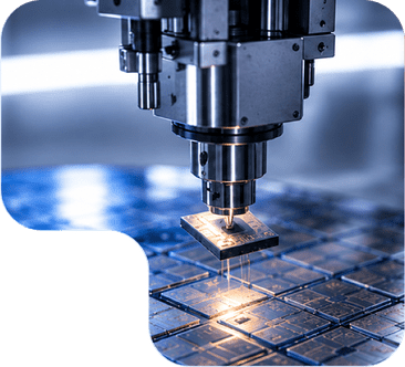
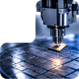
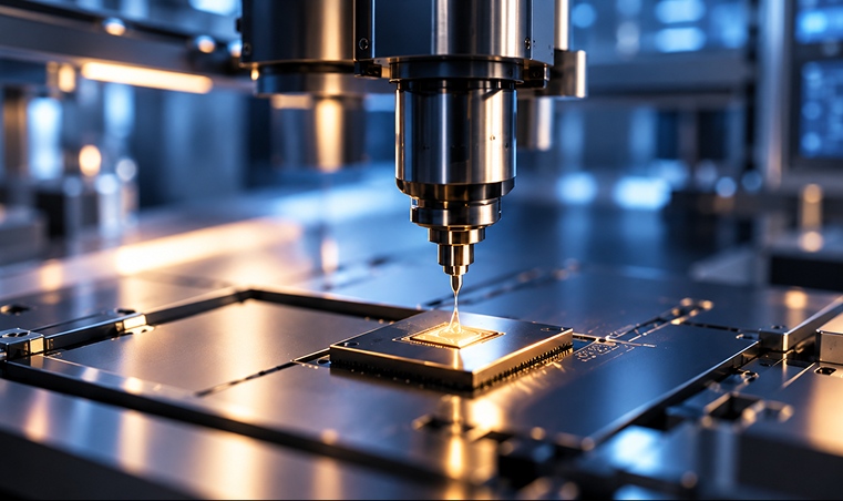
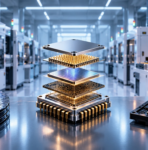
High-density flip chip bonding for superior electrical performance, reduced parasitics, and compact form factors in advanced IC packages.

SYSTEM-IN-PACKAGE MANUFACTURING
From substrate design through volume production - advanced SiP manufacturing with 3D die stacking, flip chip assembly, wire bonding, and hermetic sealing at India's only dedicated advanced packaging facility.
PACKAGING EXPERTISE
izmomicro provides comprehensive semiconductor packaging services spanning the full product lifecycle. Our capabilities cover substrate design, die attach, wire bonding, flip chip assembly, encapsulation, testing, and qualification - all under one roof at our ISO 9001:2015-certified facility in Bangalore.
FEATURED PRODUCTS
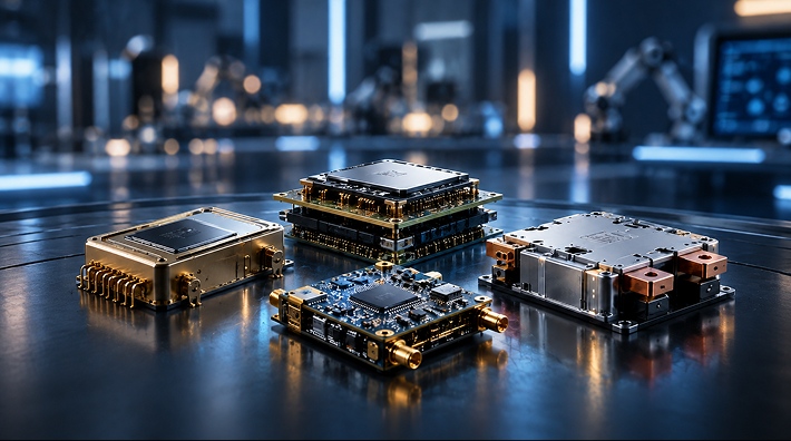
From space-grade 3D SiP modules achieving 64× footprint reduction to hermetically sealed packages for military applications, our products are proven in the field.
PRODUCT CATEGORIES
A comprehensive portfolio of standard and custom package formats, from single-chip carriers to complex multi-chip modules.
TECHNOLOGY & PROCESS
State-of-the-art equipment and specialized processes for high-reliability semiconductor packaging.
Purpose-built for high-reliability semiconductor and photonics packaging, izmomicro's advanced manufacturing infrastructure combines a Class 1000 cleanroom, precision assembly systems, specialized packaging equipment, and controlled process environments.

PROCESS CAPABILITIES
Specialized process technologies enabling high-reliability packaging for the most challenging applications.
High-density flip chip bonding for superior electrical performance, reduced parasitics, and compact form factors in advanced IC packages.
Multi-level die stacking (3D IC) integration for maximum functional density, enabling dramatic footprint reduction in space-constrained systems.
Specialized packaging for micro-electro-mechanical systems requiring zero-stress die attach, environmental protection, and reliable mechanical interfaces.
Expert handling of ultra-thin and mechanically sensitive dies with specialized tooling and processes to maintain structural integrity.
MIL-STD hermetic packaging for military, space, and high-reliability applications requiring long-term environmental protection and moisture resistance.
Precision optical component integration, including fiber alignment, lens mounting, and optoelectronic assemblies for optical communication and sensing applications.
MANUFACTURING CAPABILITIES
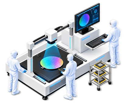
Our ISO 9001:2015-certified facility houses a Class 1000 cleanroom with automated die attach, thermosonic bonding, flip chip placement, molding and encapsulation, and full electrical and environmental test capabilities.
DESIGN CAPABILITIES
Advanced simulation and analysis capabilities supporting every aspect of package design and validation.
Designs, LTCC, HTCC, and Thermally Enhanced substrate designs for optimized signal integrity and reliability.
Signal Integrity and Power Integrity analysis ensuring clean signal transmission and stable power delivery at high frequencies.
Heat transfer simulation and thermo-mechanical stress analysis for device operation at extreme temperature environments.
Electromagnetic interference and compatibility analysis ensuring designs meet stringent electromagnetic compatibility standards.
GET STARTED
Partner with izmomicro for advanced IC packaging and SiP manufacturing. From initial package design and simulation through volume production, our team delivers the expertise and infrastructure to bring your semiconductor products to market.


