
Silicon Photonics

Silicon Photonics
Packaging


Beyond the Limits of Copper
Traditional copper interconnects are reaching fundamental bandwidth and power-density limitations. As data center bandwidth demands surge past 800G and beyond, electrical interconnects face insurmountable walls in signal integrity, power consumption, and thermal dissipation.
Silicon photonics replaces copper with light, enabling orders-of-magnitude improvements in data throughput at a fraction of the energy cost. However, realizing these gains requires solving deeply complex packaging challenges.
- Sub-micron alignment precision for fiber arrays and waveguides
- Thermal expansion mismatch between heterogeneous materials
- Co-packaging electronic and photonic dies without compromising either
Where Photonics Meets Industry
Silicon photonics is transforming five key sectors where optical performance, bandwidth density, and energy efficiency are non-negotiable.


From Die Attach to Final Test
Our photonic packaging workflow is engineered for precision at every stage, with dedicated equipment and processes for each assembly step.
Precision Die Attach
High-accuracy die placement with eutectic and epoxy bonding for photonic and electronic dies on common substrates. Placement accuracy within ±5µm for initial positioning.
Wire Bonding & Interconnect
Fine-pitch wire bonding and flip-chip assembly for high-density electrical connections between photonic and electronic components. RF-optimized routing.
Active Optical Alignment
Sub-micron precision alignment of fiber arrays and waveguides with real-time optical feedback and UV-cure fixation. <2 dB insertion loss per channel.
Test & Validation
Custom optical characterization: insertion loss, return loss, polarization-dependent loss, and spectral response across all channels at operating wavelengths.
What Sets Our Photonic Packaging Apart
End-to-end photonic packaging capabilities built on decades of advanced semiconductor assembly experience.
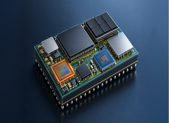
Heterogeneous SiP Integration
Multi-die assembly combining silicon photonic dies, III-V laser sources, and electronic ASICs into a single cohesive package.
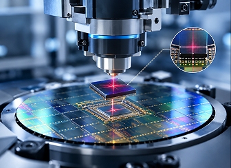
Sub-Micron Active Alignment
Real-time optical feedback alignment systems for fiber arrays and waveguides, achieving less than 2 dB insertion loss per channel.
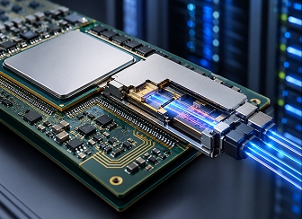
Co-Packaged Optics (CPO)
Photonic engines integrated with switch ASICs on a common substrate for next-generation data center architectures.

Class 1000 Cleanroom
ISO 9001:2015 certified assembly environment with full traceability for every photonic package produced.

Co-Packaged Optics for Data Centers
Eliminates the transceiver bottleneck by placing photonic engines directly adjacent to switch ASICs, slashing power per bit by up to 50% while enabling 51.2T switch bandwidth and beyond.
Our packaging supports multi-channel fiber I/O with low-insertion-loss attachment optimized for high-radix, spine-leaf topologies.
Exclusive Industry Partner - IIT Madras CPPICS
As the exclusive industry partner of the Centre for Programmable Photonic Integrated Circuits and Systems (CPPICS) at IIT Madras, izmomicro holds a unique position at the intersection of photonics research and industrial-scale packaging. This partnership enables joint development of next-generation photonic technologies, with izmomicro providing the packaging infrastructure to translate laboratory breakthroughs into manufacturable products.
Collaborative Research Areas
-
Programmable Photonic Processors (FPPGA)
Field-programmable photonic gate arrays enabling reconfigurable optical signal processing for telecom switching, RF filtering, and neural network inference
-
Quantum & AI-Driven Photonic Integration
Advanced packaging for quantum photonic circuits and AI-accelerated photonic systems, including entangled-photon sources and programmable linear optical networks
-
Silicon Photonics for Telecom & Computing
High-speed coherent transceiver packaging, co-packaged optics for hyperscale data centers, and photonic interposers for chiplet-based computing architectures
Photonic Chip Packaging Initiative
Advancing Next-Generation Photonic Processors
Discuss Your Silicon Photonics Project
Whether you're developing a silicon photonic transceiver, co-packaged optics module, or a novel photonic integrated circuit, our team provides end-to-end packaging support from design consultation through volume manufacturing.
-
Photonic circuit design-for-packaging consultation
-
Prototype assembly with sub-micron alignment
-
Custom optical test & characterization protocols
-
Mid-volume to production-scale manufacturing
-
IP-secure Class 1000 cleanroom environment