
Advanced Packaging for AI Accelerators Powering the Next Era of High-Performance Computing
Advanced Packaging for AI Accelerators: Powering the Next Era of High-Performance Computing
The semiconductor industry is entering a decisive transition. As Moore’s Law slows, traditional transistor scaling alone can no longer deliver the performance, efficiency, and scalability demanded by modern AI accelerators. In this new landscape, advanced packaging technologies have emerged as the primary driver of system-level innovation.
AI workloads today are increasingly constrained by memory bandwidth, I/O latency, and power and thermal limitations. Training large language models and running inference at scale require rapid data movement between compute and memory, often across multiple silicon domains. Addressing these challenges has shifted the industry’s focus toward heterogeneous integration and chiplet-based architectures, where packaging plays a central role in overall performance.
Chiplets and Heterogeneous Integration: Redefining AI System Design
Rather than relying on monolithic dies, leading AI accelerator designs now integrate specialized chiplets—compute, memory, and I/O—within a single package. This approach enables greater design flexibility, improved yield, and faster innovation cycles. However, the true advantage lies in how these chiplets are connected.
Technologies such as 2.5D interposers, CoWoS (Chip-on-Wafer-on-Substrate), and 3D packaging allow chiplets to communicate with far higher bandwidth and lower latency than traditional PCB-level connections. As a result, advanced packaging has become inseparable from processor architecture, directly influencing performance, power efficiency, and thermal behavior.
Market Momentum Behind Advanced Packaging
The rapid adoption of advanced packaging is reflected in its market growth. Advanced packaging for AI chips is projected to grow at a CAGR of 45.5% between 2024 and 2030, nearly five times faster than conventional semiconductor segments. In parallel, the global chiplet market is expected to reach USD 157.23 billion by 2030, driven by AI, high-performance computing (HPC), and data-center demand.
Ecosystem investments reinforce this momentum. TSMC continues to scale CoWoS capacity to approximately 90,000 wafers per month, supporting next-generation AI accelerators. ASE has committed over USD 1 billion toward advanced packaging capacity expansion, while ASML has introduced dedicated tools for 3D integration, accelerating the industry’s shift toward stacked and hybrid architectures.
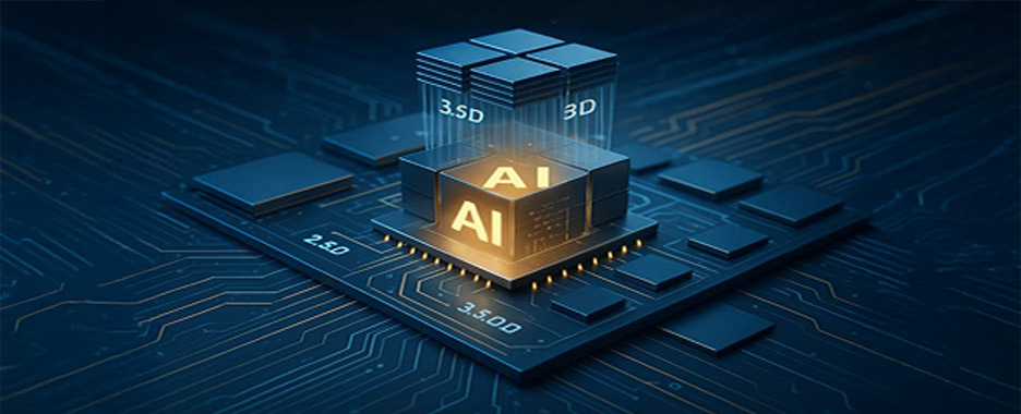
From 2.5D and 3D to 3.5D Hybrid Architectures
The evolution of packaging architectures is already visible in commercial products. AMD’s MI300X AI accelerator combines 3D SoIC with 2.5D CoWoS, demonstrating how tightly integrated memory and compute can significantly improve performance per watt. Looking ahead, the upcoming AMD MI400 series is expected to push further into 3.5D hybrid integration, enabling even denser, more power-efficient designs.
These developments highlight a fundamental change: packaging innovation is now delivering greater performance gains than transistor scaling alone.
Our Perspective: Engineering Advanced Packaging for AI at Scale
We view advanced packaging and 3D integration as strategic enablers for the future of AI computing. Our approach focuses on helping customers translate packaging complexity into competitive advantage by supporting:- Architecture design for heterogeneous, chiplet-based AI accelerators
- Migration from 2.5D and 3D packaging to 3.5D hybrid architectures
- Co-optimization of performance, power, and thermal efficiency
- Accelerated time to market through robust assembly and advanced test solutions
Advanced packaging is no longer an extension of Moore’s Law—it is the foundation upon which the next generation of AI accelerators will be built. If you are evaluating chiplet strategies or planning your next AI accelerator platform, we invite you to a conversation. Together, we can engineer packaging solutions that push computing performance beyond today’s limits.
Blog Titles
- Why Silicon Photonics Shifts...
- Smaller, Smarter, and Faster...
- Advanced Packaging: The New...
- Why Co-Packaged Optics...
- Co-Packaged Optics: From...
- Advanced Packaging for AI Accelerators...
- Co-Packaged Optics: The New Backbone...
- Advanced Packaging: The Bridge Between...
- First Silicon Bring-Up Starts with Packaging...
- Engineering the Future: Addressing Core...