
Why Silicon Photonics Shifts the Real AI Performance Bottleneck to the Package
Why Silicon Photonics Shifts the Real AI Performance Bottleneck to the Package
Custom silicon is rapidly becoming the competitive edge in AI. As models grow larger and workloads become more demanding, organizations are building purpose-designed AI CPUs, TPUs, NPUs, accelerators, and HBM-attached compute to gain performance advantages. But many teams uncover a critical challenge far too late in the design cycle: the package is not separate from the processor — it is part of it.
In advanced AI systems, performance doesn’t stop at the die. It is ultimately determined by how efficiently signals, power, thermals, and interconnects travel through the package and into the system. As silicon photonics enters mainstream AI architectures, this reality becomes even more pronounced. Optical interconnects promise massive bandwidth and lower latency, but they also raise the bar for packaging precision, thermal control, and integration strategy.
Where AI and Silicon Photonics Designs Begin to Break Down
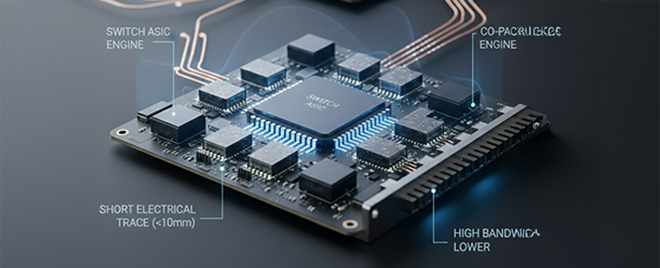
Modern AI platforms are no longer simple, monolithic chips. They rely on dense chiplet architectures, high-bandwidth memory stacks, advanced interposers, and increasingly, silicon photonics for die-to-die and system-level connectivity. The true limitations often emerge when:- Signal integrity across the die, interposer, and substrate isn’t closed early, impacting both electrical and optical links
- Power delivery noise forces frequency derating, reducing compute and I/O performance
- Thermal gradients create hotspots, affecting reliability and photonic component stability
- Chiplet, HBM, and photonic integration requires ultra-tight routing and planarity, leaving little margin for late-stage fixes
The Case for Chip–Package Co-Design
To meet the demands of next-generation AI systems, leading teams are adopting a chip–package co-design approach. Instead of designing the chip first and "fitting” it into a package later, architecture, floor planning, and packaging decisions are developed together.At izmomicro, we engage with design teams early — during system definition and floor planning — to ensure that chip, photonics, and package work as a unified system from day one. This upstream collaboration reduces risk and enables predictable performance outcomes.
Our co-design capabilities include:
- Substrate and interposer design optimized for high-bandwidth electrical and optical integration
- Signal integrity, power integrity, and thermal modeling to validate performance before tape-out
- Chiplet, HBM, and silicon photonics attach integration, balancing electrical, optical, mechanical, and manufacturing constraints
- DFM and reliability engineering to ensure smooth transition from first silicon to volume production
Engineering Performance Before Tape-Out
As silicon photonics becomes a cornerstone of AI infrastructure, success depends on designing beyond the die. Treating the package as a first-class design element eliminates bottlenecks early and dramatically improves the likelihood of achieving performance targets on first silicon.
If you’re building custom AI silicon — especially with chiplets, HBM, or photonics in the mix — let’s connect. izmomicro can help accelerate your roadmap and ensure performance is engineered into the system right from the start.
Blog Titles
- Why Silicon Photonics Shifts...
- Smaller, Smarter, and Faster...
- Advanced Packaging: The New...
- Why Co-Packaged Optics...
- Co-Packaged Optics: From...
- Advanced Packaging for AI Accelerators...
- Co-Packaged Optics: The New Backbone...
- Advanced Packaging: The Bridge Between...
- First Silicon Bring-Up Starts with Packaging...
- Engineering the Future: Addressing Core...