
Advanced Packaging The New Governor of AI and HPC Performance
Advanced Packaging: The New Governor of AI and HPC Performance
For decades, progress in AI and high-performance computing (HPC) was driven by transistor scaling. Smaller nodes, faster clocks, and denser logic defined competitive advantages. That model is reaching its limits. Today, advanced packaging has become the true governor of AI and HPC output, power efficiency, and delivery timelines.
A clear market signal underscores this shift. MetaX’s nearly 3,000× oversubscribed IPO, raising approximately US$586 million, reflects growing recognition that differentiation has moved beyond the die. Performance no longer stops at silicon. It is shaped by how compute, memory, power, thermals, and interconnects come together inside the package.
Why Packaging is New the Bottleneck
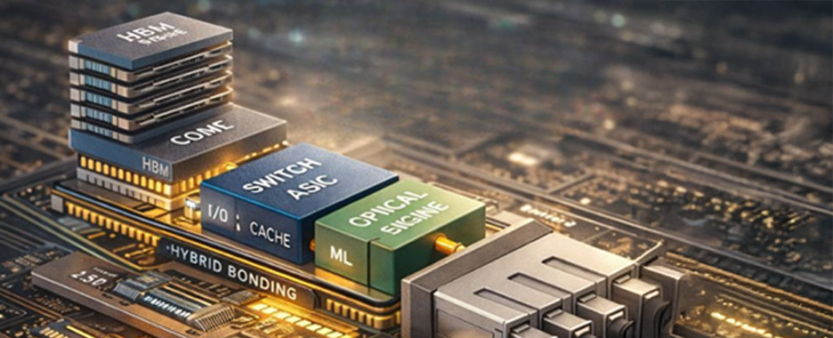
- Memory proximity and energy efficiency Modern AI workloads are constrained by data movement, not raw compute. By placing High Bandwidth Memory (HBM) next to compute using 2.5D interposers or 3D stacking, accelerators achieve multi-terabytes per second of bandwidth at far lower picojoules per bit than off-package DRAM. This proximity enables higher real-world performance within tight power envelopes.
- Chiplets at scale Chiplet-based architectures are now mainstream, enabled by UCIe and proprietary die-to-die links. Combining compute, I/O, cache, and specialty accelerators improves yield and design flexibility. However, these benefits depend on fine-pitch routing, tight skew control, known-good-die flows, and advanced assembly precision. Packaging complexity increases rapidly as chiplet counts grow.
- Power delivery and thermals as first principles Rising current density and stacked memory push package-level power delivery networks, warpage control, thermal interface materials, lids, and vapor chambers into the critical path. In many AI systems, sustainable performance is now limited by package thermal resistance rather than silicon capability.
- Manufacturability and test
Yield is no longer owned by the foundry alone. It is shared across HBM attach, interposer assembly, substrate quality, and system-level test (SLT). This elevates the importance of OSAT process control, advanced test, and reliability screening in determining shipment volumes and time to market.
Technologies Shaping the Next Phase
Several advanced packaging technologies are defining the future of AI systems:- 2.5D integration using large silicon interposers, high-layer ABF substrates, and advanced RDL/fan-out
- 3D stacking and hybrid bonding for logic–cache–memory integration
- High-efficiency PDNs and next-generation thermal materials
- Early co-packaged optics, as rack-scale I/O emerges as the next scaling wall
Asia—and India—Matter More Than Ever
Advanced packaging capacity has become strategic. Availability of HBM stacks, interposers, ABF substrates, hybrid-bonding tools, and advanced test increasingly gates global AI system deliveries.
While Asia dominates this ecosystem, India’s expanding OSAT and ATMP push is timely. Advanced-packaging-focused providers, including players like izmomicro, can plug into global AI supply chains through capabilities such as HBM attach, 2.5D/3D assembly, substrate and RDL co-design, system-level test, and reliability qualification (HTOL/HAST).
The Takeaway
AI performance and deployment timelines are now fundamentally packaging problems. The winners will pair strong compute architectures with secured capacity across HBM, interposers, substrates, and test, backed by deep co-design across foundry, OSAT, and system teams. In this AI era, advanced packaging is no longer the backend—it is the backbone.
Blog Titles
- Why Silicon Photonics Shifts...
- Smaller, Smarter, and Faster...
- Advanced Packaging: The New...
- Why Co-Packaged Optics...
- Co-Packaged Optics: From...
- Advanced Packaging for AI Accelerators...
- Co-Packaged Optics: The New Backbone...
- Advanced Packaging: The Bridge Between...
- First Silicon Bring-Up Starts with Packaging...
- Engineering the Future: Addressing Core...