
Revolutionizing Space Technology: Advanced Semiconductor Packaging for a Leading Space Agency
Revolutionizing Space Technology: Advanced Semiconductor Packaging for a Leading Space Agency
Introduction
In aerospace and satellite applications, size, weight, and reliability are paramount. A leading space agency faced limitations with its 8” x 8” PCB-based camera system: large, heavy, and inefficient for modern payloads.
izmomicro engineered an advanced System-in-Package (SiP) using substrate stacking and custom packaging. The result was a compact 3” x 3” SiP—an 85% reduction in size—that improved performance, efficiency, and scalability for future satellite payloads.
The Problem: PCB Limitations
The legacy PCB-based system posed several issues:
- Large footprint (8” x 8”), consuming valuable payload space.
- Heavy design, increasing launch costs.
- Integration challenges, as conventional PCBs struggled to combine multiple dies, wire-bonded devices, and packaged components in a small footprint.
In space, every gram and cubic millimeter matters. A radical redesign was essential.
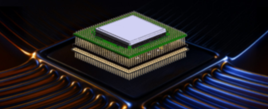
The Solution: SiP with Custom PGA Packaging
izmomicro replaced the bulky PCB with a System-in-Package (SiP) architecture:
- Size reduction – from 8” x 8” PCB to 3” x 3” SiP.
- Custom Pin Grid Array (PGA) – developed for high pin-count connectivity and mechanical strength.
- Die-level integration – combined bare dies and packaged devices within the substrate for higher density and superior performance.
This paradigm shift enabled compact, lightweight, and high-reliability payload electronics for the client.
Key Engineering Challenges
Designing such a dense, mission-ready package came with hurdles:
- Stacked substrate design – multiple dies and wire bonds required precise stacking to avoid performance degradation.
- Mixed integration – embedding packaged devices and bare dies together demanded advanced layout planning.
- Wire-bonded FPGA base – routing beneath the FPGA without creating thermal hotspots required innovative strategies.
- Shared pin utilization – pins had to serve dual roles for substrate connectivity and I/O, adding complexity.
Engineering Approach
izmomicro applied fine-line circuitry (3/3 mil traces) and advanced simulations:
- Optimized power & ground planes ensured stable current distribution.
- Signal & Power Integrity (SI/PI) analysis minimized crosstalk, noise, and voltage fluctuations.
- Thermal validation ensured reliable operation in extreme aerospace conditions.
- Future-ready design – a second-generation version will leverage silicon interposers to simplify stacking and enhance integration.
- The parts were manufactured at our state-of-the-art class 1000 Cleanroom IC Packaging facility in Bangalore.
Results & Impact
The SiP-based design achieved:
- 85% reduction in size – from 8” x 8” PCB to 3” x 3” package.
- Weight savings, reducing launch costs.
- High integration, combining multiple dies, FPGA, and packaged devices in one compact system.
- Performance efficiency, with high-speed signaling maintained through SI/PI optimization.
- Reliability for aerospace, ensuring stable operation under mission-critical payload conditions.
For the space agency, this meant greater payload efficiency, flexibility in system design, and readiness for next-generation satellite cameras.
Broader Implications
This case highlights how System-in-Package technology is transforming aerospace and defence electronics:
- Miniaturization without compromise in performance.
- Lower weight, critical for cost-sensitive payloads.
- Future scalability, enabling integration of AI/ML processors, sensors, and communication modules.
izmomicro’s collaboration with this leading space agency underscores the role of semiconductor packaging innovation in enabling advanced space exploration.
Conclusion
izmomicro’s custom SiP with fine-line circuitry and substrate stacking redefined the client’s camera payload design—achieving compactness, reliability, and scalability. As the aerospace industry pursues lighter, smarter, and more efficient systems, innovations like this will drive the next generation of satellite payloads and mission-critical applications. izmomicro’s work not only solved today’s design challenge but also set a new benchmark for the future of aerospace electronics.
Blog Titles